
//php echo do_shortcode(‘[responsivevoice_button voice=”US English Male” buttontext=”Listen to Post”]’) ?>
Intel has established a manufacturing partnership with Elon Musk’s corporate portfolio, including Tesla, SpaceX, and AI firm xAI. The project, named Terafab, aims to build a semiconductor fabrication plant in Austin, Texas.
In a public statement, posted on X, Intel confirmed it will work with the companies to “design, fabricate, and package ultra-high-performance chips at scale”. The chipmaker stated the collaboration will “help refactor silicon fab technology” to support advances in AI and robotics. Intel CEO Lip-Bu Tan characterized the effort as a “step change in how silicon logic, memory, and packaging will get built in the future.”
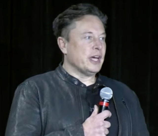
Elon Musk has indicated the project is necessary because the semiconductor demand across his companies is slated to far outstrip the supply it can get from current partners, which include Nvidia, Samsung, and TSMC. The Texas facility targets an eventual output of one terawatt of computing power annually.
Restructuring manufacturing and silicon supply chain
The current semiconductor supply chain relies on a globally distributed model. Wafers are frequently fabricated in Taiwan, integrated with memory in South Korea, and packaged in Southeast Asia.

By Bluetooth SIG 04.09.2026

By MRPeasy 04.01.2026

By Stefan Drouzas, Senior Application Marketing Manager at Rohm Semiconductor GmbH 03.31.2026
Terafab proposes a consolidated approach, locating design, lithography, fabrication, memory integration, and advanced packaging within a single 100-million-square-foot campus at the Giga Texas site. This colocation is designed to reduce the logistical latency of international shipping, allowing engineers to test and revise lithography masks within the same facility.
Intel’s contribution to the project relies on its 18A process node, which incorporates a gate-all-around transistor design and a backside power delivery network. More critically for the supply chain, Intel brings its advanced packaging capabilities, including embedded multi-die interconnect bridge and Foveros 3D stacking technologies.
These packaging methods allow for the integration of logic and memory chiplets and serve as a domestic alternative to TSMC’s chip-on-wafer-on-substrate (CoWoS) lines, which currently face extended backlog periods.
The manufacturing lines are structured around specialization rather than a broad product catalog. Approximately 20% of the capacity is allocated to the AI5 and AI6 architectures. These processors focus on edge inference and energy efficiency to power Tesla’s autonomous driving systems, the proposed Cybercab fleet, and the Optimus humanoid robot program.
The remaining 80% of the compute output is designated for space-based applications, specifically the D3 chip. This radiation-hardened processor is designed for deployment within SpaceX satellite constellations, aligning with xAI’s objective to establish orbital data centers that utilize the vacuum of space for thermal management and continuous solar power.
To manage internal logistics across the site, The Boring Company is constructing subterranean tunnels beneath the Texas campus. This underground transit system is intended to automate material transport while minimizing surface-level vibrations that can disrupt sensitive extreme ultraviolet lithography equipment.
Equipment constraints and manufacturing goals
Scaling the facility introduces structural constraints within the upstream supply chain. Advanced node fabrication requires extreme ultraviolet (EUV) lithography tools manufactured by ASML. ASML’s global production capacity is currently just over 50 EUV systems annually, with long-term projections slightly exceeding 100 tools per year.
Adrien Sánchez, a senior market and technology analyst at Yole Group, told EE Times about the equipment bottleneck. “ASML shipped just 48 EUV systems in 2025, and its order book is fully allocated to TSMC, Samsung, and Intel through 2027,” Sánchez stated. Because Terafab lacks confirmed ASML orders, it faces procurement challenges as a new market entrant.
Sánchez observed that this dynamic underscores the necessity of the partnership. “Rather than building a greenfield fab from scratch and waiting years for equipment, Terafab can leverage Intel Foundry’s existing 18A process technology, equipment allocations, and packaging infrastructure,” he said. “In other words, Terafab is likely more an Intel fab expansion with Tesla, SpaceX, and xAI as anchor customers, rather than a standalone manufacturing venture.”
The 18A process node, which utilizes a gate-all-around transistor design and a backside power delivery network, has recently seen yield stabilization near 65% at Intel’s Arizona facilities, providing a technical foundation for the expansion.
Memory component logistics
Beyond logic processors, the facility faces supply requirements for memory components. “Our estimate of the eventual wafer volumes needed to fill the demand of Terafab would have 10 million wafers per month just for memory,” John Lorenz, director of computing and memory at Yole Group, told EE Times. “This is 5× the current production of DRAM.”
Incorporating memory fabrication introduces further complexities. Lorenz expressed skepticism regarding an independent approach to memory production. “Terafab is years from producing anything,” he said. “Memory manufacturing requires entirely separate expertise that neither Tesla, SpaceX, nor Intel possesses. I doubt that the Terafab could produce its own memory without some partnership from the incumbents.”
Regarding the broader market impact, Sánchez added that the concentrated demand from Terafab adds a demand signal to an already tight memory market. “The real pricing risk isn’t Musk building his own DRAM, it’s the eventual capacity overshoot when all these new fabs come online around 2028–2029.”
Raw material dependencies
Locating the facility in Texas provides a specific supply chain advantage concerning raw materials, particularly high-purity helium. Helium is a cooling agent used in advanced lithography and packaging processes.
Furthermore, Asian foundries rely heavily on imports from the Gulf Cooperation Council region, a supply line that experienced production outages in early 2026. The U.S. produces a significant portion of the world’s helium from domestic reserves in Texas, Wyoming, Kansas, and Oklahoma.
Lorenz noted this geographic advantage but cautioned about other resource dependencies. “Building in Austin may help on the helium front, as the U.S. produces almost half of the world’s helium,” he stated. “However, bare silicon wafers are mostly coming from Asian suppliers, and the water and power needs of semiconductor manufacturing at this scale will not be trivial either.”
Competitive shifts in the foundry market
The partnership alters the dynamics of the contract foundry market. Tesla currently sources semiconductors from TSMC and Samsung. The Terafab project introduces a domestic alternative.
Stephen Ezell, VP at the Information Technology and Innovation Foundation (ITIF), analyzed the competitive implications. “This announcement represents a very significant win for Intel as it seeks to build a complementary foundry business (i.e., making chips for ‘fabless’ clients) alongside its core chipmaking business and to compete against leaders in the field like TSMC,” Ezell told EE Times. “This will bolster Intel’s ability to manufacture chips focused on AI and mobility applications.”
While the project may not pose an immediate technological challenge to TSMC’s 70% market share, it presents specific complications for Samsung Electronics. Market researchers suggest Samsung may experience a near-term surge in orders from Tesla to bridge the supply gap during the Texas facility’s construction phase. However, once Terafab becomes fully operational, Samsung risks losing a high-volume anchor customer for its advanced process nodes.
For Intel, the agreement functions as an anchor contract for its developing external foundry services. Sánchez of Yole Group assessed the strategic value for Intel. “Terafab is first and foremost a breakthrough for Intel Foundry,” he stated. “Terafab now adds Tesla, SpaceX, and xAI as further anchor customers, giving Intel Foundry the credibility it has been chasing for years.”
The partnership also provides a platform to demonstrate Intel’s advanced packaging capabilities, such as embedded multi-die interconnect bridge (EMIB), which allows for the integration of logic and memory chiplets. This serves as an alternative to TSMC’s CoWoS packaging lines, which are currently operating at full capacity.
Lorenz explained the strategic positioning. “TSMC’s advanced packaging is capacity-constrained and concentrated in Taiwan,” he said. “Hyperscalers need a second source, and Intel’s EMIB technology, manufactured on U.S. soil, can fill that gap. Here, Terafab serves as a high-profile proof of execution.”
Financing and geopolitical context
Financing the physical infrastructure and equipment procurement requires substantial capital. Analysts calculated that achieving the one-terawatt capacity would require capital expenditures ranging from $5 trillion to $13 trillion over the project’s lifespan, noting this would require the processing of 22.4 million advanced logic wafers annually.
To generate liquidity, SpaceX acquired xAI in an all-stock merger, creating an entity valued at $1.25 trillion. Following the merger, SpaceX filed draft registration documents for an initial public offering. The offering seeks a public market valuation of up to $2.0 trillion and aims to raise between $50 billion and $80 billion, with a mandated 30% allocation reserved strictly for retail investors.
The partnership aligns with U.S. government efforts to localize semiconductor manufacturing. The Trump administration previously negotiated a deal to acquire an equity stake in Intel to secure the company’s business.
This arrangement brought total recent federal investments to $11.1 billion. Securities filings indicate the U.S. government held 8.4% of Intel’s shares outstanding as of March 20, 2026. This domestic coordination aims to secure the supply chains for silicon utilized in aerospace and transportation infrastructure, mitigating exposure to trans-Pacific trade disruptions.
See also: